Perfect. But let’s talk brass tacks. Before you start fiddling with schematics or sourcing parts, there’s a critical question that could make or break your launch:
Do you really need a custom PCB, or will a development board do the job?
This single decision could save (or cost) you months of time, thousands of dollars, and your sanity. Let’s break it down.
What’s the Difference Between a Dev Board and a Custom PCB?
A dev board (short for development board) is a ready-to-use circuit board designed for fast prototyping and development. Think ESP32, STM32 Nucleo, Arduino, you’ve probably used one already.
In contrast, a custom PCB is built from scratch based on your product’s exact requirements. From layout to power optimization to component placement, it’s your hardware, your rules.
When a Dev Board is All You Need
You don’t need a custom PCB for everything. In fact, forcing one too early can stall your progress. Here’s when a dev board makes perfect sense:
You’re still validating your core idea
Your BOM has fewer than 20 components
It’s just a proof-of-concept or MVP
Off-the-shelf pinouts and I/O match your use case
Size, power, and ruggedness aren’t critical yet
Example: Testing a basic IoT sensor with Wi-Fi? Use an ESP32 dev board and get your readings out fast.
When Do You Need a Custom PCB?
Now you’re entering product territory, reliability, optimization, and scale matter.
Here’s when a custom PCB is a no-brainer:
You’re building a commercial product (not a demo)
Your form factor doesn’t fit standard dev boards
You need power efficiency (e.g., battery-powered devices)
You’re integrating multiple modules (Wi-Fi + BLE + MCU)
You need to consider EMI shielding, thermal control, or antenna tuning
You’re preparing for pilot runs or mass production
Quick reality check: If you’re shipping more than 100 units with dev boards, you’re burning money and asking for production nightmares.
The Harsh Truth: You Can’t Scale with Dev Boards
Dev boards are great for hacking ideas, lab demos, or weekend experiments. But the second you try to scale:
You end up Frankensteining multiple boards
GPIO conflicts show up out of nowhere
Power delivery becomes a mess
Firmware gets tied to the quirks of the board. You need structure, reliability, and control, and that only comes with a custom PCB.
How to Transition from Dev Board to Custom PCB, Without the Burnout
Most teams hit a wall here. Designing a PCB from scratch sounds intimidating. Circuit Tree your shortcut to pro-grade hardware design.
– Upload your design requirements – Select your processor, sensors, and interfaces – Get auto-generated schematics and PCB layout in minutes – Skip manual routing headaches and focus on building
Try Circuit Tree’sdesign automation engine now and experience how simple custom PCB development can be.
Dev Board vs Custom PCB: Decision Table
Question
If Yes
Am I just testing a concept?
Use a Dev Board
Is this a real product headed to users?
Go Custom PCB
Do I care about power, form factor, or thermal management?
Go Custom PCB
Am I experimenting or learning?
Use a Dev Board
Would I be confident showing this to a client/investor?
If not → Go Custom
Final Thoughts
Choosing between a dev board and a custom PCB isn’t just about tech. It’s about strategy.
In the early days, keep it lightweight. Move fast. But when you start seeing traction, you need to own your stack, hardware included.
If you’re ready to go from prototype to product,Circuit Tree is the fastest and smartest way to build boards that are actually production-ready.
IoT devices are small, smart, and everywhere. From wearable health monitors to industrial sensors, they’re redefining how the physical world talks to the digital one. But here’s the kicker: mostIoT hardware fails not because of bad code or weak connectivity, but because of poor board design, particularly in IoT PCB design.
If you’re building IoT hardware, read this before you even think of clicking “Start New Project” on your design tool. Because a few wrong decisions in the schematic or layout stage can kill your product before it even boots up.
This guide will provide essential advice on effective IoT PCB design.
Understanding the Essentials of IoT PCB Design
Let’s break it down.
1. Power Isn’t Just a Section on Your Schematic, It’s the Foundation
Most IoT boards are powered by batteries or low-power supplies. That means your power design isn’t just about “will it work?” It’s about “will it work for months without dying?”
Use wide traces for power rails. Undersizing them creates voltage drops that ripple across sensitive components.
Place decoupling capacitors right next to the power pins of your ICs. Not “somewhere close” we mean millimeters away.
Don’t route power under high-speed lines. You’ll unintentionally create parasitic coupling and noise.
And please, simulate your power distribution if your board is going into production.
Most importantly, don’t treat power integrity like an afterthought. For low-power IoT boards, it’s the difference between battery life that lasts 6 weeks or 6 months.
2. Wireless Isn’t Plug-and-Play, It’s Sensitive, and Demanding.
Let’s get one thing straight: your wireless module will not “just work” if your layout is sloppy.
IoT devices often rely on Bluetooth, Wi-Fi, LoRa, or LTE. Here’s how to avoid killing your signal before your product even launches:
Leave the ground plane under the antenna area untouched. No vias, no traces, no copper pours.
Keep high-speed digital traces away from RF sections. No crossing paths.
Use impedance-controlled traces for any RF lines. Guesswork doesn’t fly when you’re pushing GHz-level signals.
Don’t enclose antennas in tight metal cases unless you’ve tested the effect. Your enclosure could become your worst enemy.
Bad RF layout is one of the top reasons engineers get stuck in product delays. And if you’re using pre-certified modules, a bad layout can still invalidate certification. Yes youcan fail compliance even with a certified part if you layout it wrong.
3. Shielding Isn’t Just for High-End Devices. It’s for Every Device That Works in the Real World
Electromagnetic interference (EMI) is a silent killer in IoT hardware. Even your own components can sabotage each other.
Use grounded copper pours around noisy areas (like DC/DC converters or clock circuits).
Keep analog and digital grounds separate, then join them at a single point (star grounding) if needed.
Avoid trace stubs in high-speed nets. These act like unwanted antennas.
And yes, if you’re designing for an industrial or automotive environment, consider physical shielding. It might add cost, but it’s cheaper than failed field deployments or recalls.
4. Placement: It’s Not Art. It’s Engineering
You don’t get bonus points for packing your board like a puzzle. In IoT design, component placement directly affects performance.
Separate power, digital, analog, and RF regions clearly. Keep them functionally isolated.
Place crystal oscillators close to their associated ICs, with short, matched traces.
Orient polarized components in a uniform direction across the board to simplify inspection and reduce errors.
Good placement makes routing easier, signal integrity better, and testing faster. Sloppy placement? It snowballs into an unmaintainable mess.
So…How Do You Avoid All This Trouble Without Spending 4 Weeks in Layout Spiral?
That’s where Circuit Tree steps in.
We built Circuit Tree because we’ve been on the other side latenights, broken boards, rushed re-spins, and missed release windows. Circuit Tree automates your schematic, component selection, and layout, using verified engineering rules that understand power, wireless, and EMI from the ground up.
It’s not just drag-and-drop, it’s design intelligence built from decades of hardware experience.
Here’s what it does:
Selects the right components for your application
Auto-generates schematics, including power and RF sections
Handles placement and routing with functional awareness
Outputs a ready-to-manufacture board you can trust from the first spin
Startups, enterprises, and solo engineers use it to move faster, design smarter, and get first-time-right hardware, every time.
You’ve got a brilliant product idea. Maybe it’s a smart home device, a wearable gadget, or an IoT sensor that could change everything. But there’s one massive roadblock standing between your vision and reality: you need to design a PCB.
Suddenly, you’re drowning in technical jargon. Schematics. Component libraries. Signal integrity. Routing constraints. It feels like you need a decade of electrical engineering experience just to get started.
What if we told you there’s a way to skip all that complexity and go straight from your idea to a production-ready circuit board in just three simple steps?
Welcome to Circuit Tree.
The Traditional Hardware Design Nightmare
Picture this: You’re a product manager with zero electronics background, tasked with bringing a new IoT device to market. Your first meeting with the hardware team goes something like this:
Engineer: “First, we need to create the schematic. That’ll take 2-3 weeks.” You: “What’s a schematic?” Engineer: “It’s like a blueprint showing how all the electronic components connect.” You: “Can’t we just… describe what we want?” Engineer:sighs “It doesn’t work that way.”
Endless research into component selection and compatibility
Trial and error with layout and routing rules
The Bottleneck Problem
Every single hardware project gets stuck in the same places:
Finding the right components for your specific needs
Creating custom schematics from scratch
Ensuring your design actually works before manufacturing
Navigating the maze of design rules and constraints
The Time-to-Market Killer
While software teams ship updates daily, hardware teams are still stuck in 6-month design cycles. Your competitors launch while you’re still figuring out capacitor values.
Meet Circuit Tree: Your Intelligent Hardware Assistant
Imagine having a seasoned hardware engineer who could instantly understand your product requirements and generate a complete, manufacturable PCB design in minutes instead of months.
That’s exactly what Circuit Tree does.
Circuit Tree is an intelligent assistant built specifically for product managers, startup founders, and anyone who needs professional PCB designs without the traditional engineering overhead. It’s like having GitHub Copilot for hardware design – except instead of suggesting code, it’s building complete circuit boards.
How It Actually Works
Instead of forcing you to learn complex design software, Circuit Tree uses AI to:
Automatically generate schematics based on your requirements
Select optimal components from a vast, curated library
Handle placement and routing according to industry best practices
Produce manufacturable designs that pass quality checks
The best part? You never have to draw a single schematic or learn what a “via” is.
Check out this quick demo to see it in action:
The 3-Step Method: From Idea to Production
Here’s how you can go from a napkin sketch to ordering prototype boards in less than 48 hours:
Step 1: Define Your Use Case (5 Minutes)
Head toapp.circuit-tree.com and describe what you want to build. You can submit:
Plain English descriptions (“I need a WiFi-enabled temperature sensor”)
Want to go straight to prototypes? Circuit Tree can handle that too; we’’ll manufacture and ship your boards directly, with full aftersales support and post-PCB processing services.
Real Products Built With Circuit Tree
MicroPython STM32 Development Board
A startup needed a custom development board for their IoT platform. A traditional approach would have taken 3 months and required hiring specialized engineers. With Circuit Tree: 2 weeks from concept to working prototypes.
ESP32 Gateway Project
An industrial IoT company needed a ruggedized gateway device with specific connectivity requirements. Circuit Tree generated a design that passed all environmental tests on the first revision.
ESP32 Rapid Development Click Board
A startup needed a compact, WiFi-enabled board for quick prototyping. Circuit Tree generated a custom ESP32-based design that fit into their click-board form factor with all components placed and routed.
Why Circuit Tree Actually Works
1.Engineering Intelligence
Circuit Tree’s AI engine is trained on years of real-world engineering insights and successful designs. It knows what works and what doesn’t, saving you from costly mistakes.
2.Massive Component Library
Access to thousands of pre-validated components with real-time availability and pricing. No more hunting through datasheets or worrying about obsolete parts.
3.First-Time-Right Approach
The platform is designed to produce manufacturable designs that work correctly on the first revision. No expensive respins or debugging cycles.
4.Real-World Validation
Every design follows industry-standard practices and is validated by experienced engineers before delivery.
Who Circuit Tree Is Perfect For
1.Product Managers and Non-Technical Founders
You understand markets and user needs, but hardware design isn’t your expertise. Circuit Tree bridges that gap without forcing you to become an electrical engineer.
2.Startup Teams on Tight Deadlines
When time-to-market is everything, Circuit Tree eliminates the traditional hardware bottlenecks that kill momentum.
3.R&D Teams Exploring New Concepts
Need to quickly validate hardware concepts without dedicating months to design work? Circuit Tree accelerates your innovation cycles.
4.Hobbyists Ready to Scale
You’ve outgrown breadboards and Arduino shields, but professional PCB design feels overwhelming. Circuit Tree makes the transition seamless.
5.Anyone Facing Resource Constraints
Don’t have a full-time hardware engineer? Can’t justify hiring specialized talent for a single project? Circuit Tree provides expert-level design capabilities on demand.
Design Hardware at Software Speed
Here’s the revolutionary part: Circuit Tree makes hardware development as agile as software development.
Instead of waterfall processes with long feedback cycles, you can:
Iterate rapidly on design concepts
Test ideas quickly with fast prototyping
Scale seamlessly from prototype to production
Focus on your product, not the underlying technology
It’s like having a hardware team that works at software speed, without the overhead of building and managing that team.
Circuit Tree doesn’t just generate PCB designs – it transforms how you think about hardware development. It removes the barriers that have kept hardware innovation slow and expensive, making it accessible to anyone with a great product idea.
Ready to turn your idea into reality? VisitCircuit Tree and see how fast you can go from concept to prototype. Your next breakthrough product is just three steps away.
Stop waiting for hardware expertise you don’t have. We are here to take care of the rest. Start building the products your customers actually want.
In the fast-paced world of electronics development, time is more than money—it’s your competitive edge. After years of working closely with engineering teams, we’ve heard the same challenge repeatedly: PCB design creates bottlenecks that slow down innovation.
That’s why we’re excited to announce our game-changing new application.
Our team has developed an intelligent PCB automation solution that transforms what traditionally takes days into a process completed in under an hour.
Automated PCB Flow diagram
Through advanced algorithms, we’ve created a system that handles placement and routing with minimal human intervention while maintaining complete design integrity. For more details visit AutoCuro
What makes this different?
Unlike conventional PCB design tools that require extensive manual work, our application intelligently analyzes your requirements and constraints to generate optimal layouts automatically. This isn’t just another iteration of existing tools—it’s a fundamentally different approach to PCB creation. The system is particularly valuable for teams juggling multiple designs across various tools. No more waiting for specialized engineers to become available or dealing with design inconsistencies between team members.
Be among the first to transform your design process
We’re currently opening limited beta access to selected partners who understand the value of dramatically accelerated design cycles. Early adopters will have direct input into future features and priority support from our expert team.
Interested in cutting your PCB design time by up to 75%?
Visit our contact page to express your interest in the beta program. Our team will reach out personally to qualified applicants. The future of PCB design is here—and it’s measured in minutes, not days.
Here is one more blog where the ESP32 Gateway bring up is displayed along with a video.
The ESP32 Gateway Board described here would be tested and its bring-up would be shown. Here is the block diagram of the board:
Block diagram gateway
Bringup Steps
Here are some of the bring-up steps followed for testing:
1. Visual inspection: Quick check to ensure that all components are soldered as per the orientation and visual shorts exist.
2. Power and clock check: Quick power test on the PCB to check for open short test. Using the multimeter to quickly test the 3.3V and 5V supply. The clock output from the oscillator was tested at 50Mhz.
3. USB connection: USB cable was connected to the J10 port. 5V and 3.3V supply was good on the board and coming at test points. Checked on oscilloscope to measure voltage ripple which is under 5%.
4. Reset check: The reset was asserted and de-asserted by TPS3895 as expected.
5. USB to UART connections: An external board was used to connect the ESP32 UART port to USB Port on the board.
6. ESP32 detection: The factory programmed ESP32 comes with the Wifi stack and can be easily detected as the WIFI host with the name ESP32. If the ESP32 is out of reset it would show esp32 wifi LAN which can be connected to. It again indicates it is alive and functional.
7. LED programming: Ardunio was selected to test the board as it is easy to program and most of the drivers are easily available. Programmed the LED program to test the led and also testing the programming sequence of JP1.
8. Switch detection: Next quick program which detects switch press and led lighting up.
9. Mounting the Click board: Mounted the ADXL345 accelerometer from Mikro Electronica on the click connector. The LED on accel click switches on and the supply stays stable for 3.3v and 5v.
10. Testing of i2c interface: Detected the device at 0x1d and 0x51. Read through the register values and moved the boards to check the accelerometer output.
i2c_scanner_Gatway
11. Testing of spi interface: Changed the Mikroe Accell click board to spi mode and tested the spi operation on the board using ESP32 module.
12. Testing other examples with esp32: The board was tested with other software examples specified at the Sparkfun website to check for power, operation, and functionality.
13. Testing of LAN8710 device. The device was detected using the MDC/MDIO pins. Ethernet cord was connected to the port and the activity led blink was observed. More tests are underway on the board.
Here is the link to the video of the board displaying power-up status detecting i2c devices on board and on module. The next video would contain some additional tests with ethernet port. Arduino code used with the esp32 rapid development click board is available at link.
In this blog, we describe how are our boards are hardware tested after prototypes are available. This testing is done to ensure that the boards designed work and work as per requirements.
The ESP32 click Board described here would be tested and its bring-up would be shown. Here is the block diagram of the board:
ESP32 Block diagram
Bringup Steps
Here are some of the bring-up steps followed for testing:
1. Visual inspection: Quick check to ensure that all components are soldered as per the orientation and visual shorts exist.
2. Power check: Quick power test on the PCB to check for open short test. Using the multimeter to quickly test the 3.3V and 5V supply.
3. USB connection: USB cable was connected to the J10 port. 5V and 3.3V supply was good on the board and coming at test points. Checked on oscilloscope to measure voltage ripple which is under 5%.
4. Reset check: The reset was asserted and de-asserted by TPS3895 as expected.
5. FT232 Driver detection: The device was quickly found on the laptop and the driver was easily found on the web. This indicates that the USB to UART device ft232 is functioning correctly.
6. ESP32 detection: The factory programmed ESP32 comes with the Wifi stack and can be easily detected as the WIFI host with the name ESP32. If the ESP32 is out of reset it would show esp32 wifi LAN which can be connected to. It again indicates it is alive and functional.
7. LED programming: Ardunio was selected to test the board as it is easy to program and most of the drivers are easily available. Programmed the LED program to test the led and also testing the programming sequence of JP1.
8. Switch detection: Next quick program which detects switch press and led lighting up.
9. Mounting the Click board: Mounted the ADXL345 accelerometer from Mikro Electronica on the click connector. The LED on accel click switches on and the supply stays stable for 3.3v and 5v.
10. Testing of i2c interface: Detected the device at 0x1d. Read through the register values and moved the boards to check the accelerometer output.
i2c_device_detected
11. Testing of spi interface: Changed the Mikroe Accell click board to spi mode and tested the spi operation on the board using ESP32 module.
12. Testing other examples with esp32: The board was tested with other software examples specified at the Sparkfun website to check for power, operation, and functionality.
13. Testing of battery charging and functionality. The battery of 220mA was connected to the battery connector and charged. The voltage was measured on the port. Shortly afterward the battery-powered operation was tested.
Bring up and the testing of the board were fun and quite enriching as with each board it brings pleasure to see circuit tree platform getting mature.
Here is the link to the video of the board displaying power-up status reading accelerometer data from the module. Arduino code used with the esp32 rapid development click board is available at link
Ever wondered how you would support the Arduino platform bring up when your custom board is different than the ExpressIF devC board. If you have just started working on the platform here are the top three challenges you would come across:
1. Arduino pin numbers mapping with board pins.
Ardunio maps the pins based on the GPIO’s of the ESP32. Many a time young engineers get stuck when they create software and it does not work.
2. Program and reset the assertion sequence on the board.
ESP32 needs the GPIO0 set to low so that ESP32 can enter in the program state. This is done at power-up and after programming, the GPIO0 pins need to be driven high.
Failed_to_connect_to_ESP32
3. Pins numbers different than Ardunio standard pins.
Ever wondered if the i2c pins or other function pins are different than the Arduino defined pins on board. For instance, esp32 assumes that the i2c pins are set at 5, 6 by default always. Most of the young engineers do wonder how they would connect the pins which in case of esp32 click board was on 22 and 23. For i2c the code attached can be used to quickly scan the i2c bus.
USB to UART cable connector for connecting FTDI USB to UART cable.
Onboard regulators of 3.3v/5V along with control logic
Switch and LED’s to provide status.
4 layer design
The board has been designed autonomously by Circuit Tree application. This design has been added in Example 4 in app-circuit-tree.com and can be customized/modified with any changes desired.
Here are some of the screenshots of the top/bottom SVG renderings.
All_layers_gateway
esp32 gateway svg Top_Side
esp32 gateway svg Bot_layer
Fabricated Board
Assembled Board
Bring-up test is underway for the board. So far initial tests show no electrical failures. We did miss on the silkscreen but that is why we need to automate more so that errors are minimized.
Design files and Arduino test code is uploaded at the Github link.
Everybody likes rapid development kit. These boards should be easy to interconnect to a number of boards/shields and offer firmware to jump-start to start testing the idea.
What better to have click modules designed by Mikro-electronica which offers more than 500+ boards to connect any type of peripheral.
esp32 from express-if is another popular board that offers wifi/Bluetooth along with a number of peripherals bus to connect to a variety of devices.
Combining these two functions on the board boosts a number of different ideas that can be implemented with this board.
So introducing our new board named esp32 rapid development click board. The board has been designed using Circuit tree app autonomously except for some placement change and silkscreen updates which were done manually.
Here are some of the key features of the board:
ESP32D-WROOM Module used.
USB/Battery powered board
On-Board UART to USB function for debugging and programming.
Onboard regulators of 3.3v/5V along with control logic
Switch and LED’s to provide status.
Screenshots:
Here are some of the screenshots of the top/bottom SVG renderings.
esp32_click_module_all
esp32_click_module_Top_Side
esp32_click_module_back
esp32 rapid development board-PCB Fabrication -Top side
esp32_click_board_assembled
Design files Arduino test code are available at Github.
There is much more planned fun along with the board which would be shared in upcoming blogs.
This board is available on sale from our website.
Designing a board gives a lot of satisfaction and fills you with motivation to keep going. The happiness and motivation that we got from the project were boosted much more as it was not only the successful board bring up but it was the Circuit Tree application that was also tested.
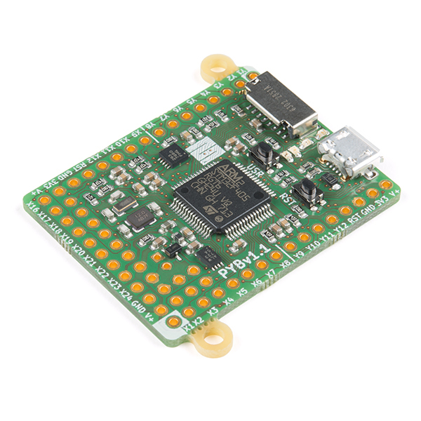
We are big fan of Python as it is extensively been used on most of our development tasks. One of our colleagues mentioned to create a third board using circuit tree having micro-python running on it. That sounded like a cool idea.
We wanted to build the board having feature set similar to the micro python 1.1 board. The additional constraint was to even have the interfaces and the dimensions the same.
Using Circuit Tree the design was loaded using command line entry through schematic. The Circuit Tree application autonomously completed these different activities:
Interconnected the components specified in the requirement.
Selected power, clock, reset components
Selected discrete values needed by different components as per the electrical requirement.
Generated the clean and error free schematic
Accepted the board boundary which was the micro python form factor.
Completed board placement. This placement had to be modified as some some components were placed far off. So human intervention was done here.
Generated a two layer PCB design on it own. All the pcb routing, plane creation, Thick traces routing , length matching was autonomously. Here Human intervention was introduced to redo some traces. Human intervention was introduced to ensure that the design was correct.
Gerber files were generated by the app after the silk screen was updated by engineer working on the program.
Using BOM component links the components were ordered. So yes it was minimal human intervention and feels good looking at the task circuit tree application is now able to undertake.
It is a two layer design with pictures below displaying svg of all layers, bottom and top layers.
All_layers_pyboard1.1
Bottom side pyboard1.1
Top side pyboard1.1
And here is the PCB Fabricated using circuit tree application design:
Fabricated board
The board is now under pcb assembly. Waiting patiently to get the boards so that we can load the micro python the board.
The PCB has been in India and this is the third board from us. Lots of learnings along the way.
We dream for the day when we are able to design complex boards (6+ layers, 400+ components including BGA components) using Circuit Tree application under 3 hours of effort.
If board design is a pain point for you write back to us what you would like us to solve.


 So…How Do You Avoid All This Trouble Without Spending 4 Weeks in Layout Spiral?