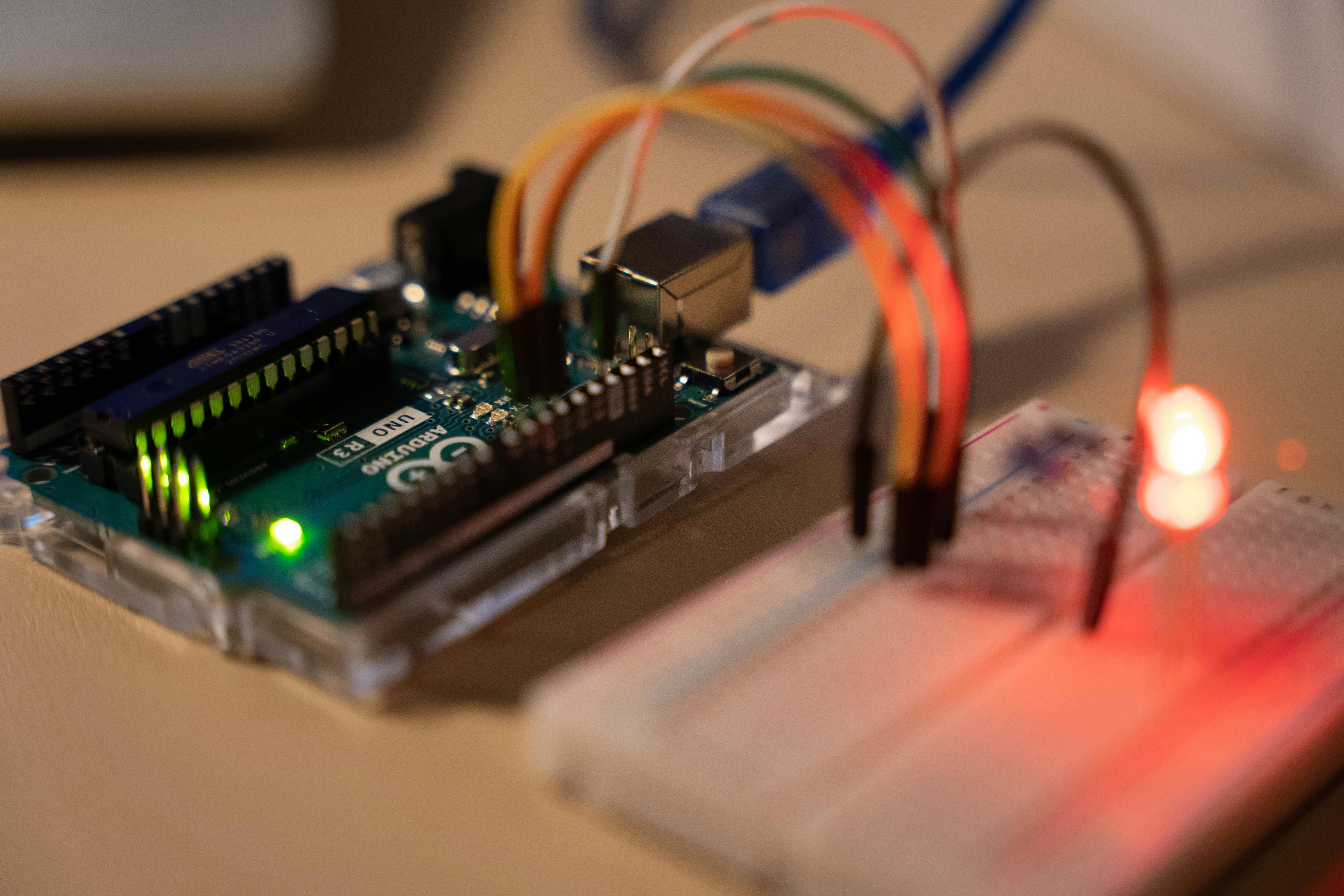
IoT devices are small, smart, and everywhere. From wearable health monitors to industrial sensors, they’re redefining how the physical world talks to the digital one. But here’s the kicker: most IoT hardware fails not because of bad code or weak connectivity, but because of poor board design, particularly in IoT PCB design.
If you’re building IoT hardware, read this before you even think of clicking “Start New Project” on your design tool. Because a few wrong decisions in the schematic or layout stage can kill your product before it even boots up.
This guide will provide essential advice on effective IoT PCB design.
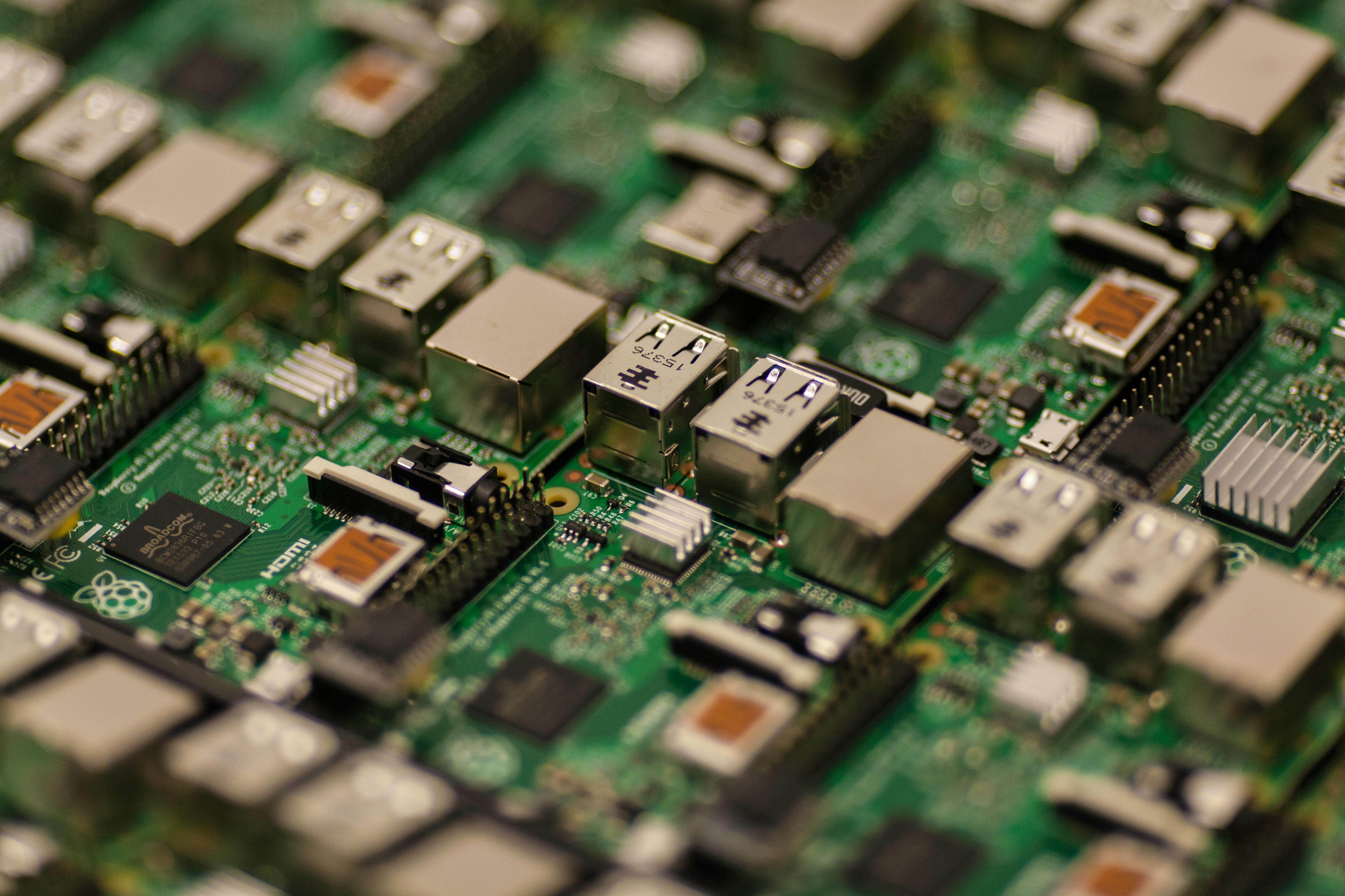
Understanding the Essentials of IoT PCB Design
Let’s break it down.
1. Power Isn’t Just a Section on Your Schematic, It’s the Foundation
Most IoT boards are powered by batteries or low-power supplies. That means your power design isn’t just about “will it work?” It’s about “will it work for months without dying?”
- Use wide traces for power rails. Undersizing them creates voltage drops that ripple across sensitive components.
- Place decoupling capacitors right next to the power pins of your ICs. Not “somewhere close” we mean millimeters away.
- Don’t route power under high-speed lines. You’ll unintentionally create parasitic coupling and noise.
- And please, simulate your power distribution if your board is going into production.
Most importantly, don’t treat power integrity like an afterthought. For low-power IoT boards, it’s the difference between battery life that lasts 6 weeks or 6 months.
2. Wireless Isn’t Plug-and-Play, It’s Sensitive, and Demanding.
Let’s get one thing straight: your wireless module will not “just work” if your layout is sloppy.
IoT devices often rely on Bluetooth, Wi-Fi, LoRa, or LTE. Here’s how to avoid killing your signal before your product even launches:
- Leave the ground plane under the antenna area untouched. No vias, no traces, no copper pours.
- Keep high-speed digital traces away from RF sections. No crossing paths.
- Use impedance-controlled traces for any RF lines. Guesswork doesn’t fly when you’re pushing GHz-level signals.
- Don’t enclose antennas in tight metal cases unless you’ve tested the effect. Your enclosure could become your worst enemy.
Bad RF layout is one of the top reasons engineers get stuck in product delays. And if you’re using pre-certified modules, a bad layout can still invalidate certification. Yes you can fail compliance even with a certified part if you layout it wrong.
3. Shielding Isn’t Just for High-End Devices. It’s for Every Device That Works in the Real World
Electromagnetic interference (EMI) is a silent killer in IoT hardware. Even your own components can sabotage each other.
- Use grounded copper pours around noisy areas (like DC/DC converters or clock circuits).
- Keep analog and digital grounds separate, then join them at a single point (star grounding) if needed.
- Avoid trace stubs in high-speed nets. These act like unwanted antennas.
And yes, if you’re designing for an industrial or automotive environment, consider physical shielding. It might add cost, but it’s cheaper than failed field deployments or recalls.
4. Placement: It’s Not Art. It’s Engineering
You don’t get bonus points for packing your board like a puzzle. In IoT design, component placement directly affects performance.
- Separate power, digital, analog, and RF regions clearly. Keep them functionally isolated.
- Place crystal oscillators close to their associated ICs, with short, matched traces.
- Orient polarized components in a uniform direction across the board to simplify inspection and reduce errors.
Good placement makes routing easier, signal integrity better, and testing faster. Sloppy placement? It snowballs into an unmaintainable mess.
 So…How Do You Avoid All This Trouble Without Spending 4 Weeks in Layout Spiral?
That’s where Circuit Tree steps in.
We built Circuit Tree because we’ve been on the other side late nights, broken boards, rushed re-spins, and missed release windows. Circuit Tree automates your schematic, component selection, and layout, using verified engineering rules that understand power, wireless, and EMI from the ground up.
It’s not just drag-and-drop, it’s design intelligence built from decades of hardware experience.
Here’s what it does:
- Selects the right components for your application
- Auto-generates schematics, including power and RF sections
- Handles placement and routing with functional awareness
- Outputs a ready-to-manufacture board you can trust from the first spin
Startups, enterprises, and solo engineers use it to move faster, design smarter, and get first-time-right hardware, every time.
You bring the intent. We build the board. Learn more at www.circuit-tree.com.
Final Word:
Hardware is hard, but it doesn’t have to be painful.
When you’re building IoT hardware, your PCB layout isn’t “just another task.” It’s the foundation of performance, reliability, and user trust.
So before you build your next IoT product, make sure your design process is as smart as your product.
And if you want to do it right, do it fast, and get it first-time-right, start with Circuit Tree.